 A.I.
A.I.
Hardware · Chips
Blackwell
Blackwell is a family of NVIDIA AI chips. The NVIDIA GB300 NVL72 puts 72 Blackwell Ultra GPUs and 36 Grace CPUs in one rack. A GPU, or graphics processing unit, is the chip that does the AI math, and a CPU is the general-purpose processor that runs everything around it. Rubin is the next NVIDIA family. Meta's purchase is on the Meta stack.
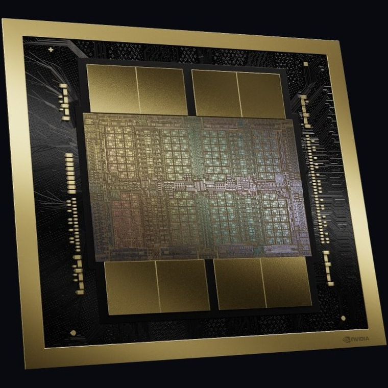
One Blackwell Ultra GPU
NVIDIA's Blackwell Ultra datasheet, dated October 2025, gives figures for one Blackwell Ultra GPU as NVIDIA configures it in the GB300 NVL72 rack below (NVIDIA, Blackwell Ultra datasheet). These are NVIDIA's own figures. NVIDIA prints the FP8 figure as sparse only.
| Figure | One Blackwell Ultra GPU |
|---|---|
| FP4 Tensor Core, dense | 15 PFLOPS |
| FP4 Tensor Core, sparse | 20 PFLOPS |
| FP8/FP6 Tensor Core, sparse | 10 PFLOPS |
| GPU memory | 279 GB HBM3E |
| Memory bandwidth | 8 TB/s |
Tensor Cores are the parts of the GPU that do the matrix math behind AI. FP4, FP6, and FP8 store each number in 4, 6, and 8 bits. A PFLOPS is a thousand trillion math operations per second. Dense counts every number, and sparse counts a shortcut that skips zeros in the math, so it reads higher. HBM3E is a type of high-bandwidth memory, the fast memory stacked next to the chip. TB/s is terabytes per second.
GB300 NVL72
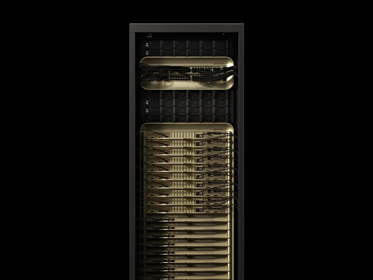
NVIDIA announced the GB300 NVL72 on 18 March 2025. It is a rack-scale system, meaning the whole server rack is built as one machine. The rack connects 72 Blackwell Ultra GPUs and 36 Grace CPUs, which are based on Arm Neoverse designs. NVIDIA says the rack acts as a single GPU built for test-time scaling, which lets a model spend more computing power while it works out an answer. NVIDIA puts its AI performance at 1.5 times the GB200 NVL72 and said partner products would start in the second half of 2025. The product page also claims 1.5 times more dense FP4 Tensor Core FLOPS and 2 times higher attention performance than Blackwell GPUs. Attention is the step where a model weighs which earlier words matter. These are NVIDIA's own claims.
| Figure | GB300 NVL72 |
|---|---|
| GPUs | 72 Blackwell Ultra |
| CPUs | 36 Grace |
| CPU cores | 2,592 Arm Neoverse V2 |
| Fast memory | 37 TB |
| GPU memory | 20 TB at up to 576 TB/s |
| CPU memory | 17 TB LPDDR5X at 14 TB/s |
| NVLink (GPU-to-GPU link) | 130 TB/s |
| FP4 Tensor Core, with sparsity | 1,440 PFLOPS |
| FP4 Tensor Core, without sparsity | 1,080 PFLOPS |
| FP8/FP6 Tensor Core | 720 PFLOPS |
| INT8 Tensor Core | 24 POPS |
| FP16/BF16 Tensor Core | 360 PFLOPS |
| TF32 Tensor Core | 180 PFLOPS |
| FP32 | 6 PFLOPS |
| FP64 and FP64 Tensor Core | 100 TFLOPS |
| Network, per GPU | ConnectX-8 at 800 Gb/s |
On the product page, Tensor Core figures count sparsity unless a figure is marked without it, the same shortcut as in the GPU table above. The second FP4 figure is the one without it. FP16, BF16, TF32, FP32, and FP64 are other number formats, and the larger ones are more precise but slower. INT8 stores whole numbers in 8 bits. A TFLOPS is a trillion math operations per second, and POPS counts whole-number operations the way PFLOPS does. NVLink is NVIDIA's wiring that lets the GPUs share work. LPDDR5X is a low-power type of memory used by the CPUs, and ConnectX-8 is NVIDIA's network card.